19 July, 2020
![]()
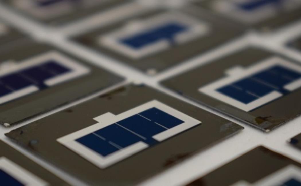
The team was able to achieve uniform perovskite coverage by using an innovative technique for depositing the perovskite onto the textured layer of silicon solar cells.
© Hou et al.
A novel technique for mass-producing better-performing perovskite-based solar cells could lay the foundations for next-generation devices that have more efficient power than currently available technologies.
Perovskite solar cell (PSC) technologies have been shown to be dramatically more efficient compared with conventional, single-crystal silicon solar cells. In particular, thin-film halide PSCs have unique characteristics that make them ideal for photovoltaics. These include structural and optoelectronic properties, such as a high degree of crystalline order, a tunable bandgap and a high optical absorption coefficient.
These properties allow them to achieve power conversion efficiencies of more than 25 percent. They also make them attractive as top cells for tandem applications that use crystalline silicon substrates and could lead to PSCs with higher efficiencies.
However, the silicon surface, which usually contains micrometer-sized pyramidal structures, must be entirely covered by the perovskite to achieve these efficiencies, but achieving this coverage has proved very challenging.
Now, Erkan Aydin and Michele De Bastiani, from the KAUST Solar Center, working with scientists from the University of Toronto, Canada, and the National Renewable Energy Laboratory, U.S., have developed an innovative technique for depositing the perovskite onto the textured layer of silicon solar cells.
The technique is scalable for mass production and also enhances the optoelectronic properties compared to conventional perovskite-silicon tandems.
“Conventional solar cells employ only one semiconductor to convert sunlight into electricity, but their theoretical efficiency is limited to around 33 percent,” explains Aydin. “By stacking two semiconductors in a ‘tandem’ solar cell, as we did, using halide perovskites and silicon, this limit can be pushed to 44 percent.”
The researchers combined a solution-processed, micrometer-thick, wide-bandgap perovskite solar cell with the pyramidal-textured layer of silicon, which filled the gaps in the silicon surface without hampering the photovoltaic properties of the perovskite and produced a tandem perovskite/silicon solar cell with an efficiency of 25.7 percent.
“Previously, the silicon surface had to be flat polished to accommodate the perovskite layer, which greatly increased the cost of mass production,” says Aydin.
The work could help to scale up the production of tandem PSCs with significantly enhanced performance, allowing researchers to work on perovskite/silicon tandem solar cells that are already the industrial standard, rather than working with platforms that cannot be mass produced.
“Our next step is to scale up our perovskite deposition technology to meet the current industrial size standards of the devices, first as a proof of concept, and then to pilot-line scale at a later stage,” says De Bastiani.