Advanced Thin Film Deposition Laboratory
Cleanroom research space featuring class 1000 and class 100 cleanroom zones with state of the art gas-phase deposition facilities. These tools allow researchers and students to carry out fundamental and applied studies related to vacuum deposited CIGS (Copper Indium Gallium Selenide) and related materials systems including rare indium and gallium metals; amorphous and microcrystalline Si; triple and multi-junction solar cell fabrication; large area (> 6"x 6") printed solar cells; photolithography; plasma etching and screen printing.
Among other highlights the cleanroom features:
- Plasma-enhanced chemical vapor deposition
- Atomic layer deposition
- UV to IR ellipsometry
- Advanced photoresist processing system
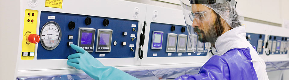
- Wet bench silicon etching and cleaning
- Fast ramping thermal processing
- Laser patterning
- Spin coating
- Large-area inkjet printing
- Scanning electron microscopy
Facilities
This multi-chamber Deposition System (Cluster Tool) is designed to deposit thin-film semiconductors (e.g., a-Si, nc-Si, p+Si, n+Si) and dielectrics (e.g., SiNx, SiOx) by PECVD, transparent conducting oxides (ITO, AZO), and metals (Al) by sputtering.
Atomic layer deposition (ALD) is a highly controlled thin film deposition method, in which a film is grown on a substrate by exposing its surface to alternate gaseous species (typically referred to as precursors).
The Oxford Instruments Inductively Coupled Plasma Reactive Ion Etch system is typically used for etching Si3N4, SiO2 and Si. The tool is load-locked and is configured to handle 4-inch wafers.
Multiple industry standard JST chemical work, etching and cleaning stations are available for processing single wafers.
The J. A. Woollam IR-VASE® spectroscopic ellipsometer combines the chemical sensitivity of FTIR spectroscopy with thin film sensitivity of spectroscopic ellipsometry.
The J. A. Woollam VUV-VASE® variable angle spectroscopic ellipsometer is ideally suited for optical characterization of lithographic thin films. It measures wavelengths from vacuum ultraviolet (VUV) to near infrared (NIR).
The DMP-3000 features a larger printable area of 300 x 300 mm with a positional accuracy and repeatability of ± 5 µm and ± 1 µm, respectively.
The DMP-5000 has a printable area of 500 x 500 mm and maintains a positional accuracy and repeatability of ± 5 µm and ± 1 µm, respectively.
This Zeiss Auriga workstation is a crossbeam high resolution SEM equipped with Focus Ion Beam (FIB) column and EDS allowing for unique imaging possibilities, advanced analytics and precise processing at a nanoscale level.
The Jipelec JetFirst 200 benchtop RTP features a temperature measurement and control system using pyrometers and thermocouples to provide accurate and repeatable thermal behavior from low to high temperatures.
The series VS screen-stencil printer offers high quality in fine-line printing of thick films, solar cells, wafers, glass, metal, etc.
The EVG101 is an advanced resist processing system that performs automated spin coating/spray coating/developing processes in a single chamber design. The EVG101 supports wafers up to 300 mm in size.
The EVG510HE semi-automated hot embossing system is designed for embossing and nanoimprinting applications.
The EVG 105 is ideally suited for softbake, post-exposure bake and hardbake processes.
The EVG620NT Semi Automated Mask Alignment System handles sizes of substrates starting from less than 5 mm up to 150 mm. It offers features, including a granite base, active vibration isolation and linear motors to meet higher precision and throughput requirements.