11 February, 2020
![]()
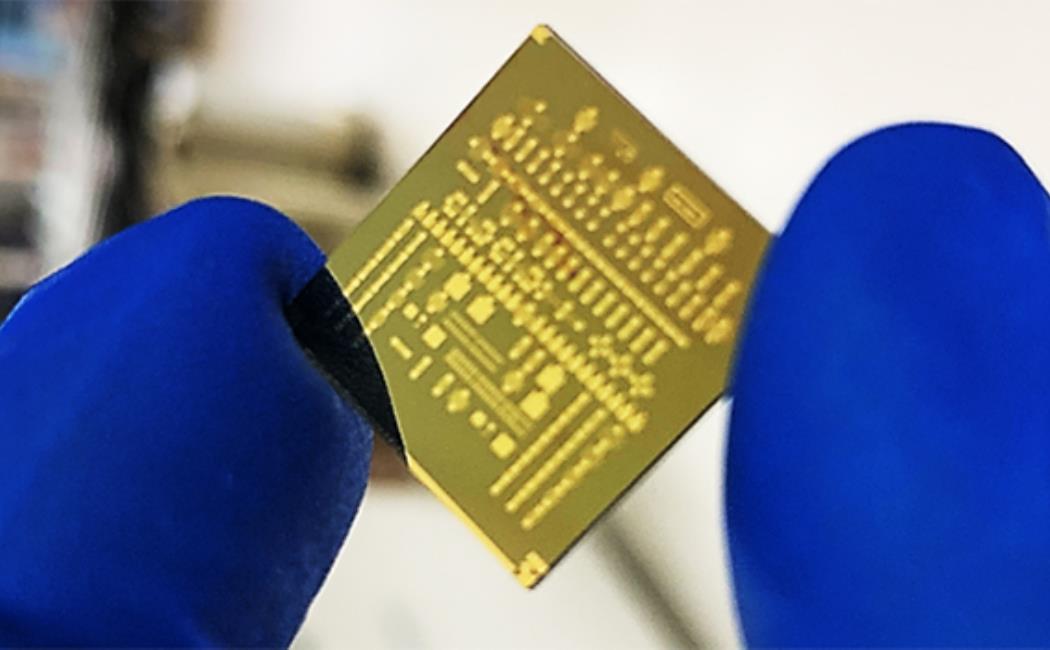
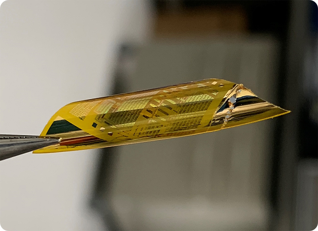
Flexible integrated circuits can be manufactured using the low-temperature, hybrid transistor technology.
© 2019 KAUST
An innovative manufacturing technique developed by KAUST researchers has led to the development of hybrid organic transistors for use in next-generation electronic displays and large-area electronics.
Thin-film transistors (TFTs) made from metal oxides have useful properties, including optical transparency and high charge-carrying capacity, and they are increasingly being used in organic light-emitting diode displays.
Currently, most TFTs are made using physical vapor deposition methods, but solution-based printing could hold promise for a simpler and more cost-effective approach. However, producing metal oxide TFTs with high carrier mobility and operating stability has proved challenging.
Led by Thomas Anthopoulos and colleagues from the KAUST Solar Center, an international team of researchers from the United Kingdom, China and Greece has made a hybrid TFT from solution-processed layers of polystyrene sandwiched between ultrathin sheets of indium oxide and zinc oxide nanoparticles.
“Much to our surprise, we discovered that the electron mobility of this hybrid TFT was very high,” explains Anthopoulos. “But more importantly, we found that the ability of the device to sustain electrical bias for a long period of continuous operation, without changing its operating characteristics, has improved dramatically.”
Previous work by Anthopoulos and colleagues had shown that TFTs made from two or more metal oxides can generate sheets of mobile electrons at the interface of the metal oxide layers. These electrons are free to move across the device, increasing its charge carrying capacity. However, structural defects present in the polycrystalline layers that form the interfaces produce election traps, altering the electrical properties of the device.
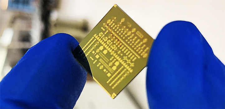
Thin-film transistors made from metal oxides have useful properties, including optical transparency and high charge-carrying capacity, and they are increasingly being used in organic light-emitting diode displays.
© 2019 KAUST
The researchers found that first inserting a polystyrene layer between the metal oxide layers and then applying an ultraviolet-ozone treatment to the layer caused the polystyrene to decompose into smaller molecular species that reacted with the oxide layers, strengthening the bonds between nanoparticles and removing some of the electron traps.
“The key to the success of our design is the incorporation of an ozone-treated polystyrene interlayer, which passivates the electron traps present on the surface/interface of the metal oxides and increases not only the electron mobility of the device but also its bias-stress stability," says Anthopoulos.
The work presents a simple, cost-effective and scalable method for fabricating TFTs for application in next-generation displays and a range of other large-area electronics.
“Next, we want to see if we can exploit the same electron trap passivation technique for different metal oxide semiconductors or other combinations of materials. I'm confident that we will identify even better-performing materials,” says Anthopoulos.